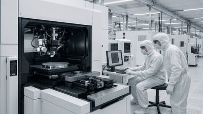
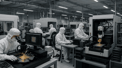
Thin film deposition sits at the core of modern semiconductor manufacturing, quietly shaping every transistor, interconnect, and memory cell. As chips become more complex and vertically integrated, the demand for high‑performance deposition equipment—especially physical vapor deposition (PVD), chemical vapor deposition (CVD), and atomic layer deposition (ALD)—has accelerated. In recent cycles, this demand has reached the point where order books for key tools are being filled well into 2027, signaling both a structural shift in capital expenditure and a sustained confidence in long‑term semiconductor growth.
This blog post explores why PVD, CVD, and ALD tools are seeing surging demand, what is driving orders to stretch multiple years ahead, and how this wave of investment ties into trends across logic, memory, power devices, and advanced packaging.
The expanding role of thin film deposition in advanced nodes
As process nodes scale, the number and complexity of thin film steps grow. Gate stacks, high‑k dielectrics, channel materials, liners, barriers, and passivation layers all rely on carefully controlled deposition. At advanced nodes, these layers must be extremely uniform, conformal, and defect‑free at nanometer scales. This pushes fabs to invest heavily in sophisticated deposition platforms capable of meeting tighter specifications.
PVD remains central for metals and some barrier layers, while CVD is widely used for dielectrics and certain structural films. ALD has moved from niche to mainstream for ultra‑thin, highly conformal coatings, particularly where aspect ratios are extreme or interface precision is critical. Together, these tools underpin the material engineering that allows transistors and interconnects to keep shrinking without sacrificing reliability.
The cumulative effect is straightforward: more layers, more demanding films, and more reliance on specialized deposition techniques translate into more tool hours and more tools per fab, driving sustained demand for equipment.
3D architectures: from FinFETs to GAA and 3D NAND
Device architectures have shifted from planar to genuinely three‑dimensional structures. In logic, FinFETs are giving way to gate‑all‑around (GAA) nanosheet and nanowire designs, which require conformal coatings around complex geometries. In memory, 3D NAND stacks have soared past hundreds of layers, with each layer requiring precise films for charge storage, control gates, and isolation.
These 3D architectures dramatically increase the importance of ALD and carefully tuned CVD processes. Conformal coverage of high‑aspect‑ratio structures is difficult to achieve with traditional methods alone. ALD’s self‑limiting surface reactions and CVD’s tailored chemistries allow manufacturers to coat narrow channels, deep trenches, and tall stacks uniformly.
As layer counts and structural complexity rise, deposition tool capacity becomes a bottleneck. Fabs respond by ordering more tools and higher‑throughput configurations, and since new lines and nodes are planned years in advance, those orders naturally extend into 2027 and beyond.
Materials innovation: high‑k, metals, and exotic films
Scaling is no longer just about shrinking features; it is increasingly about changing materials. High‑k dielectrics replace traditional oxides to maintain gate control, new metals and alloys enter interconnect stacks to reduce resistance, and exotic films are used for barrier, liner, and seed layers. Each new material often requires its own optimized deposition process and, sometimes, dedicated equipment variants.
PVD tools must handle more complex metal stacks with tight thickness and purity requirements. CVD tools are adapted for new low‑k dielectrics and stress‑engineering films. ALD platforms are tuned for emerging materials that demand atomic‑scale thickness control and perfect interfaces. Each material innovation increases process diversity and tool utilization.
Because materials roadmaps are planned several generations ahead, fabs and equipment makers coordinate long‑term capacity and capability, booking tool orders aligned with these future needs and extending the demand horizon into 2027.
Advanced packaging: redistribution layers, interposers, and chiplets
The rise of advanced packaging—2.5D interposers, 3D stacking, chiplet‑based designs—has moved thin film deposition beyond traditional front‑end fabs into back‑end and OSAT (outsourced semiconductor assembly and test) environments. Redistribution layers (RDLs), microbumps, through‑silicon vias (TSVs), and various interconnect schemes rely on precise metal and dielectric films.
PVD tools deposit metals for interconnects and bumps; CVD and ALD tools are used for insulating layers, liners, and barrier films in packaging structures. As high‑bandwidth memory, heterogeneous integration, and system‑in‑package solutions proliferate, packaging lines require more deposition capacity and higher‑quality films to match front‑end reliability and performance.
This packaging‑driven demand adds a new dimension to tool orders. Not only front‑end fabs but also advanced packaging houses are booking PVD/CVD/ALD equipment, contributing to the overall surge and stretching order backlogs further into the future.
Power and analog devices: wide‑bandgap materials and specialized films
Beyond mainstream logic and memory, power and analog devices—especially those based on wide‑bandgap materials like silicon carbide (SiC) and gallium nitride (GaN)—are expanding rapidly. Electric vehicles, renewable energy, industrial systems, and fast chargers need robust, efficient power electronics, which depend on specialized thin films for passivation, isolation, and gate structures.
CVD and ALD are particularly important for high‑quality dielectrics and interface layers in these devices. PVD continues to play a role in metal contacts and interconnects. As production of SiC and GaN devices scales up, their fabs add deposition tools to meet growing wafer volumes and tighter reliability requirements.
This sector’s growth reinforces long‑term demand: power and analog expansions tend to follow multi‑year industrial investment cycles, naturally driving tool orders that align with the 2026–2027 timeframe and beyond.
Capacity expansion and geographic diversification
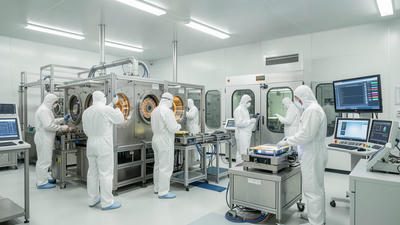
Global semiconductor manufacturing is diversifying geographically as regions pursue their own fabs and capacity expansion plans. New plants in multiple countries and existing fabs adding lines or upgrading nodes all require baseline deposition capacity. PVD, CVD, and ALD tools are part of the standard equipment set for any modern fab.
When multiple regions build out capacity simultaneously, the aggregate demand for deposition tools climbs sharply. Tool makers must plan production over several years to satisfy overlapping projects, leading to order books that cover extended periods rather than short cycles.
Geographic diversification also encourages redundancy and local resilience, which can involve additional tool purchases for backup capacity or modular expansions, amplifying the ordering momentum into 2027.
Equipment lead times and supply chain constraints
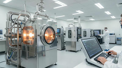
Thin film deposition tools are complex systems composed of vacuum chambers, gas delivery, RF power, temperature control, robotics, and control software. Building, testing, and qualifying these tools takes time, and many subsystems depend on specialized vendors. When demand spikes, lead times naturally extend.
Supply chain constraints for critical components—valves, pumps, power supplies, precision hardware—can further lengthen delivery schedules. To secure capacity and avoid delays in fab ramp‑ups, chipmakers place orders early and accept longer horizons for delivery.
This combination of complexity and constraints means that a surge in demand translates directly into multi‑year order books. Tool makers and customers plan on 2027 and beyond to ensure that future fabs and nodes have the deposition capacity they will need.
Technology transitions and node migrations
Node migrations—moving from older process technologies to more advanced ones—often require new deposition tools or substantial upgrades. Even if wafer capacity does not increase dramatically, the mix of tools changes as fabs adopt new materials and structures. In some cases, legacy tools cannot support required film qualities or uniformity and must be replaced.
As foundries and memory makers transition simultaneously across multiple nodes, they place concentrated orders for next‑generation PVD, CVD, and ALD tools. These transitions are typically staged over several years, with overlapping ramps and qualification phases.
Order books reflecting these transitions naturally stretch into 2027, especially when customers want to secure tool positions early to avoid bottlenecks at critical points in their roadmaps.
Increasing equipment intensity per wafer
Another structural trend is rising equipment intensity—more process steps per wafer and greater reliance on deposition at each node. Even without large jumps in wafer starts, the total number of deposition cycles per wafer has grown as stacks become more complex and multi‑patterning and multi‑layer structures proliferate.
When equipment intensity rises, existing fabs need more deposition chambers and higher throughput just to maintain capacity. This drives orders for additional tools and cluster expansions, even in the absence of new fab construction.
Because equipment intensity is tied to underlying technology evolution rather than short‑term demand, its impact on PVD/CVD/ALD tool demand is durable, supporting multi‑year ordering and investment horizons.
Competitive dynamics among equipment makers
Surging demand for deposition tools also reflects competitive dynamics among equipment vendors. Companies compete on throughput, film quality, footprint, energy efficiency, and process flexibility. As they introduce new platforms that offer improved performance, customers may choose to upgrade more aggressively, accelerating replacement cycles.
Equipment makers, in turn, invest in capacity, R&D, and support infrastructure to capture a larger share of this demand. Their sales pipelines and order books are shaped not only by industry‑wide needs but also by how quickly they can bring competitive products to market.
This competition tends to increase the overall volume of tool orders, as customers diversify their suppliers or trial new platforms alongside existing ones, all of which contributes to robust bookings into 2027.
Implications for fabs and capital planning
For fabs, surging demand and long order books mean that capital planning must be more forward‑looking. Decisions about PVD, CVD, and ALD investments now require multi‑year visibility on technology roadmaps, product mixes, and potential bottlenecks.
Fabs may choose to over‑order or pre‑order tools to build buffer capacity, especially in areas where process complexity is rising most quickly. They also need to plan for installation, training, and integration of new equipment into existing lines, recognizing that deposition tools often sit at critical junctions in workflows.
Capital planners have to balance near‑term needs with long‑term flexibility, ensuring that tool purchases made for 2027 can serve multiple generations and product families rather than being tied too narrowly to a single node.
Implications for downstream customers and markets
Downstream customers—device makers, systems integrators, and end users—may not see deposition tools directly, but they feel their effects. Adequate deposition capacity and advanced film capabilities are prerequisites for reliable product ramps and performance gains in CPUs, GPUs, memory, and power devices.
When tool demand is high and order books are full, there can be risks of delayed node introductions or constrained supply if equipment deliveries slip. Conversely, strong investment in PVD/CVD/ALD platforms supports more predictable technology rollouts and capacity expansions, which underpin roadmaps for PCs, smartphones, data centers, and automotive systems.
Understanding the health and direction of deposition tool demand can thus offer clues about the trajectory of broader semiconductor markets and the timing of new product capabilities.
Conclusion: thin film tools as quiet engines of the next semiconductor wave
The surge in demand for thin film deposition tools—PVD, CVD, and ALD—and the fact that orders are being booked into 2027 highlight their central role in the current semiconductor wave. From 3D architectures and advanced packaging to wide‑bandgap power devices and geographic capacity expansion, nearly every major trend relies on more and better thin films.
As a result, these tools have become quiet engines of progress: seldom visible outside fab walls, yet indispensable to every new node, memory breakthrough, and system innovation. The multi‑year ordering patterns we see today reflect not just a cyclical upturn, but a deeper structural shift toward more material‑intensive, vertically integrated, and geographically diversified semiconductor manufacturing—one in which thin film deposition stands at the very heart.