In the semiconductor world, photomasks sit at a critical junction between design data and physical wafers. They encode circuit patterns with nanometer precision and serve as the optical templates for lithography across logic, memory, and specialty devices. For years, high-end photomask capability has been concentrated in a handful of global clusters, making domestic fabs heavily dependent on imported masks for advanced nodes. Recently, however, localization rates in certain regions have begun to break through, driven by progress from emerging players such as Qingyi and Luwei. Their advances mark a significant shift in the balance between global and domestic supply and signal a new phase in the maturation of local semiconductor ecosystems.
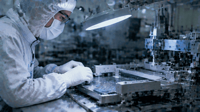
This blog post examines what a “breakthrough” in photomask localization really means, how the photomask value chain works, why it has been difficult to localize, and how companies like Qingyi and Luwei are changing the landscape. It also explores what rising localization implies for fabs, tool vendors, design houses, and broader industrial policy.
Photomasks: from design data to wafer patterns
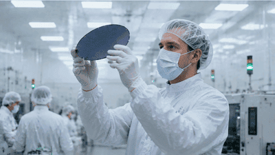
Photomasks—often simply called masks or reticles—are glass or quartz plates patterned with opaque and transparent regions that define how light or other radiation reaches the wafer during lithography. Each mask corresponds to a specific layer of the device: gates, contacts, interconnects, isolation structures, and more.
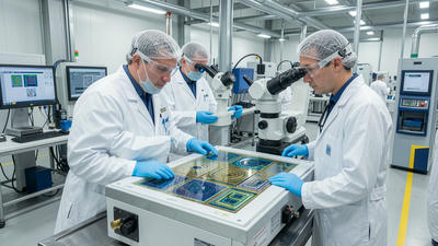
Mask production starts from design data, which is processed through optical proximity correction (OPC), resolution enhancement techniques (RET), and data preparation to account for lithography system characteristics and process distortions. The resulting data drives mask writing tools that pattern high-resolution features, followed by inspection, repair, pellicle mounting, and extensive qualification.
Because any defect or error on a mask can replicate across thousands of wafers, photomasks are both high-value and high-risk items in semiconductor manufacturing.
Why photomask localization has been difficult
Localizing photomask production is challenging for several reasons. First, mask technology is capital- and knowledge-intensive. High-end electron-beam writers, inspection systems, and repair tools are expensive and require deep process expertise to operate and maintain.
Second, mask-making demands advanced materials and processes: ultra-clean substrates, precise chrome or other absorber deposition, sophisticated resist processing, and tight control of line edge roughness and critical dimensions. Building domestic supply chains for these inputs is non-trivial.
Third, mask shops must maintain extremely low defect rates and tight schedule performance for demanding fab customers, which depends on both technical capability and operational maturity. These barriers have historically favored established mask houses in regions with long semiconductor traditions.
Localization rate: what “breaking through” means
Localization rate in photomasks refers to the share of masks that fabs source from domestic producers rather than overseas suppliers. For many years, domestic mask providers focused on mature nodes or less critical applications, with advanced masks largely imported.
A breakthrough in localization rate means domestic providers have reached a point where they can reliably supply a significant portion of masks, including more complex layers and nodes, to local fabs. This can be measured in terms of volume share, node coverage, or the number of fab lines qualified on domestic masks.
Progress by companies like Qingyi and Luwei suggests that local mask capability is moving beyond niche roles into mainstream support for critical manufacturing, marking a new phase in localization.
Qingyi and Luwei: emerging pillars of local mask capacity
Companies such as Qingyi and Luwei have invested heavily in building full-service photomask operations: from data preparation and mask design support to writing, inspection, and qualification. Their expansion typically began in mature nodes and specialty applications, then extended toward more advanced logic and memory masks.
These firms have developed expertise in handling complex OPC patterns, tight CD control, and stringent defect budgets. By working closely with domestic fabs, they have tailored their processes to local lithography toolsets and process conditions, improving compatibility and yield.
As their capabilities and track records grow, fabs become more willing to shift mask orders from overseas suppliers to these domestic players, driving localization rates upward.
Technology investments: tools and processes
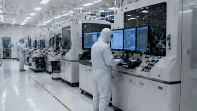
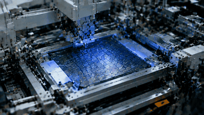
Breaking through in photomask localization requires significant capital investment. Qingyi and Luwei have deployed modern mask writers capable of handling dense, complex patterns at advanced nodes. They have added high-resolution inspection systems, repair tools, and environmental controls to manage contamination and pattern integrity.
Process flows—resist coating, exposure, development, etching—must be tuned to achieve tight tolerances in CD and uniformity. Mask cleaning and pellicle integration routines are optimized to maintain performance in high-throughput fab environments.
These technology investments create the physical backbone of domestic mask capability, anchoring localization efforts in solid manufacturing infrastructure.
Data preparation and design integration
Mask-making is not just about hardware; data preparation is equally critical. Qingyi and Luwei have built teams and software pipelines to handle OPC, RET, and mask data processing for a variety of design styles and technology nodes. This includes managing huge data volumes, aligning with lithography system parameters, and maintaining secure interfaces with design houses and fabs.
Integration with local design ecosystems is key. Domestic mask shops that understand common design practices, device architectures, and fab-specific requirements can iterate quickly on mask data to achieve desired lithography performance.
This design integration capability is a core part of photomask localization, enabling domestic providers to serve as full partners rather than just downstream producers.
Qualification with local fabs
Localization breakthroughs depend on successful qualification campaigns with local fabs. Qingyi and Luwei have worked closely with process and lithography teams to qualify their masks across multiple layers and devices. Trials involve running test lots, measuring CD uniformity, overlay performance, defect status, and yield metrics.
Once masks from domestic suppliers meet fab requirements consistently, they can be certified for production use. Over time, the number of layers and products supported by domestic masks expands, raising localization rates steadily.
These qualification processes also generate feedback that helps mask shops refine their technology, creating a virtuous cycle of improvement and trust.
Economic and strategic benefits of localization
For fabs, higher photomask localization offers several benefits. It can reduce lead times by shortening logistics chains and avoiding overseas shipping. It may ease communication and coordination around mask changes, fixes, or urgent reorders, thanks to geographic and cultural proximity.
Economically, local sourcing can reduce exposure to foreign currency fluctuations, import duties, or export controls. Strategically, relying on domestic mask providers supports national objectives around semiconductor self-reliance and resilience, especially for nodes and products considered critical.
For mask makers like Qingyi and Luwei, increased localization translates into more stable demand, closer customer relationships, and stronger positions in the domestic semiconductor value chain.
Risk management and multi-sourcing
Even as localization rates climb, fabs generally maintain multi-sourcing strategies for photomasks. Mask defects or delivery issues can impact large volumes of wafers, so relying on a single source is risky. Domestic providers become part of a diversified supplier portfolio, sometimes sharing layers or products with global mask houses.
Higher localization enables fabs to re-balance risk: they can rely more on domestic suppliers for certain nodes or layers while keeping international partners for others. This flexibility supports business continuity plans and allows fabs to respond more effectively to disruptions in any particular region.
Qingyi and Luwei’s progress thus contributes to a more resilient mask supply structure rather than a monolithic one.
Challenges that remain for domestic mask providers
Despite breakthroughs, domestic photomask providers still face challenges. Keeping pace with leading-edge nodes demands continual tool upgrades, process refinement, and staff training. Integrating new resolution enhancement techniques, supporting next-generation lithography, and handling increasingly complex patterning schemes require ongoing R&D investment.
Competitive pressure from established global mask houses persists, especially in segments where they have decades of experience and extensive portfolios. Domestic providers must differentiate on responsiveness, local integration, and cost-effectiveness while reaching technical parity.
Maintaining low defect rates across higher volumes and more layers also becomes more demanding as localization expands.
Interaction with lithography equipment localization
Photomask localization interacts closely with efforts to localize lithography equipment and process modules. Fabs using domestic or regionally sourced lithography tools benefit from mask shops that understand and optimize for those specific tool characteristics. Conversely, masks tuned primarily for global tool platforms may require adaptation for new or localized systems.
Qingyi and Luwei can play a bridging role, working with both domestic lithography tool projects and imported systems to ensure masks deliver expected performance. Their experience in local process conditions makes them valuable partners in aligning mask specs with actual tool behavior.
This interaction strengthens the broader ecosystem of localized lithography and patterning capabilities.
Impact on design and tape-out timelines
Design houses and fabless companies care deeply about mask availability and tape-out timelines. Improved photomask localization can shorten the cycle from final design data to first silicon by reducing communication overhead and shipping delays. Domestic mask providers can offer more direct feedback on data issues and help debug lithography-related problems earlier in the flow.
Closer collaboration among designers, fabs, Qingyi, and Luwei can streamline design-for-manufacturability efforts, as mask and process limitations are better understood and incorporated into design rules and OPC strategies.
Over time, this tighter loop may allow local ecosystems to iterate more quickly on new products, enhancing competitiveness beyond the mask shop itself.
Policy and industrial strategy dimensions
Photomask localization aligns naturally with industrial policies aimed at strengthening domestic semiconductor capacity. Authorities often view masks as strategic resources because of their role in translating design IP into manufacturing patterns. Supporting companies like Qingyi and Luwei through funding, infrastructure, and talent development can be part of broader semiconductor initiatives.
Policy frameworks may encourage collaboration between mask shops, universities, and research institutes to advance mask technologies, inspection methods, and data processing techniques. They can also facilitate access to critical tools and materials needed for high-end mask-making.
As localization rates break through, policymakers gain tangible evidence that domestic investment strategies are paying off in core segments of the semiconductor value chain.
Future directions: EUV and advanced patterning
Looking ahead, the frontier for photomask localization includes EUV masks and other advanced patterning technologies. EUV masks introduce new materials, multilayer structures, and defect challenges that are more complex than traditional optical masks. Localizing these capabilities requires additional tool sets, specialized inspection, and deep process expertise.
While companies like Qingyi and Luwei may initially focus on deep ultraviolet (DUV) and mature-node masks, gradual expansion into more advanced patterning segments will determine how far localization can extend into cutting-edge nodes.
Progress in these areas will further enhance the strategic value of domestic mask capacity, cementing its role in the long-term trajectory of local semiconductor industries.
Conclusion: photomask localization as a key milestone
The breakthrough in photomask localization rates, anchored by progress from companies such as Qingyi and Luwei, marks an important milestone in the evolution of domestic semiconductor ecosystems. Photomasks, once almost exclusively sourced from overseas for advanced applications, are increasingly produced locally with sufficient quality, reliability, and integration to support critical fab lines.
For fabs, this shift improves resilience, reduces certain costs and delays, and strengthens local collaborations across design and manufacturing. For mask shops, it validates years of investment in tools, processes, and expertise. As localization continues and extends into more advanced patterning domains, photomask capability will remain a central pillar of any region’s quest for greater semiconductor self-reliance and competitiveness.