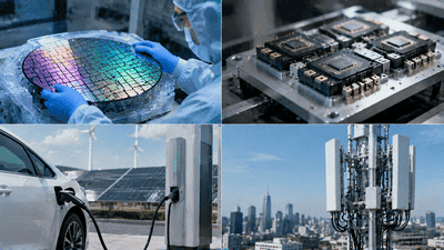
Third-generation semiconductor substrates such as silicon carbide (SiC) and gallium nitride (GaN) are reshaping power electronics, RF devices, and high‑efficiency energy systems. They are often described as a break from traditional silicon, yet silicon‑based materials have not disappeared from the picture. Instead, they have found new, strategically important roles around these wide‑bandgap substrates: as templates, integration platforms, thermal and mechanical partners, and key elements in hybrid packaging. The interplay between silicon and third‑generation semiconductors is becoming a central theme in how next‑generation devices are designed and manufactured.
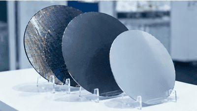
This blog post explores emerging application scenarios for silicon‑based materials in the context of third‑generation semiconductor substrates. It looks at how silicon interacts with SiC and GaN in power and RF devices, where silicon is used to enable manufacturability and reliability, and how new architectures leverage silicon to bridge the gap between advanced materials and system‑level requirements.
From pure silicon to hybrid material systems
Traditional semiconductor devices were largely built on silicon wafers with silicon‑based dielectrics and interconnects. Third‑generation semiconductors expand this picture by introducing wide‑bandgap substrates that outperform silicon in breakdown voltage, thermal stability, and switching speed. Rather than eliminating silicon, these new materials add layers to the system: silicon platforms now coexist with SiC and GaN chips in modules and packages.
Hybrid material systems integrate silicon as a complementary element, handling control logic, sensing, and interface functions while SiC or GaN devices manage power conversion or high‑frequency signals. Silicon becomes the “system substrate” upon which wide‑bandgap devices are assembled, interconnected, and cooled.
This shift from pure silicon to hybrid stacks opens many new application scenarios for silicon‑based materials in third‑generation semiconductor designs.
Silicon as a platform for GaN on Si
One of the most visible interfaces between silicon and third‑generation semiconductors is GaN on Si technology. Here, gallium nitride epitaxial layers are grown on silicon wafers, combining GaN’s wide bandgap and high electron mobility with silicon’s cost and wafer‑scale infrastructure. Silicon acts as the mechanical and thermal base for GaN devices in RF and power applications.
Developers must manage lattice and thermal mismatch between GaN and Si, using buffer layers and engineered interfaces. Silicon’s role is not just passive: its thickness, doping, and crystalline quality influence device performance, yield, and reliability. GaN on Si technologies thus represent a major application scenario where silicon‑based materials directly support third‑generation substrates.
As demand for GaN power and RF devices grows, GaN‑on‑Si approaches continue to evolve, keeping silicon central to substrate engineering.
Silicon carbide and silicon in multi‑chip modules
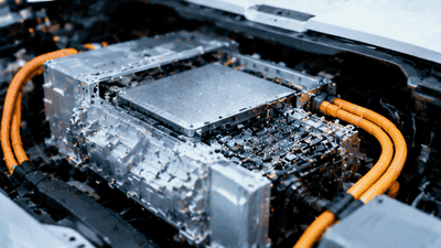
SiC substrates enable high‑voltage, high‑temperature power devices for electric vehicles, industrial drives, and energy infrastructure. In many application modules, SiC chips are co‑packaged with silicon‑based components: drivers, controllers, protection circuits, and communication interfaces. Silicon serves as the platform for digital and mixed‑signal functions that coordinate SiC power stages.
Module substrates, often built from silicon‑based materials or silicon‑compatible ceramics, provide electrical routing, mechanical support, and thermal pathways between SiC devices and system‑level connectors. Silicon’s familiarity in packaging and interconnect design allows manufacturers to integrate SiC dies without completely reinventing module structures.
This co‑existence in multi‑chip modules is a key scenario where silicon and third‑generation substrates collaborate to deliver practical, high‑volume power solutions.
Silicon interposers for heterogeneous integration
Silicon interposers—thin silicon layers with fine‑pitch interconnects—are increasingly used to assemble heterogeneous systems: mixing logic, memory, analog, and specialized chips. When third‑generation semiconductors enter the mix (for example, GaN or SiC dies in a high‑performance system), silicon interposers can provide the wiring density and mechanical structure to connect them with traditional silicon chips.
In this scenario, silicon is both a substrate and a routing medium. Through‑silicon vias (TSVs) and micro‑bumps connect diverse dies, allowing high‑bandwidth data exchange and compact layouts. Silicon interposers can help manage signal integrity and thermal paths, even when wide‑bandgap devices operate at high voltages or frequencies.
Heterogeneous integration on silicon interposers thus becomes a powerful application scenario for combining third‑generation substrates with established silicon technologies.
Silicon‑based thermal management structures
Third‑generation semiconductors excel at high‑temperature, high‑power operation, but system‑level thermal management still benefits from engineered silicon structures. Silicon’s thermal conductivity, mechanical stability, and compatibility with existing processing make it a candidate for heat spreaders, thermal vias, and integrated cooling elements in modules containing SiC or GaN devices.
Silicon‑based micro‑channel cooling, embedded thermal vias, or bonded silicon plates can help remove heat from hotspots, distributing it across larger surfaces where traditional heatsinks or liquid cooling can operate more effectively. These structures leverage silicon’s machinability and well‑understood processing to complement the thermal properties of wide‑bandgap substrates.
In advanced power modules and RF front‑ends, silicon‑based thermal management components increasingly appear alongside SiC and GaN chips as part of integrated cooling solutions.
Silicon oxides and nitrides as interface layers
Silicon‑based dielectrics such as silicon dioxide (SiO₂) and silicon nitride (Si₃N₄) remain essential in third‑generation substrate systems. They serve as passivation layers, isolation films, and interface dielectrics between wide‑bandgap materials and metal interconnects or packaging structures. These layers help control electric fields, manage surface states, and protect devices from environmental exposure.
In SiC and GaN devices, silicon‑based dielectrics may be used to shape gate structures, define isolation regions, or tune capacitances in power and RF circuits. Their processing compatibility with existing equipment and familiarity in reliability engineering make them natural choices for many interface roles around third‑generation substrates.
These applications illustrate how silicon‑derived materials continue to underpin device robustness even when the active substrate is no longer pure silicon.
Silicon in advanced packaging substrates
Advanced packaging for third‑generation semiconductors often uses silicon‑based substrates or silicon‑compatible laminates. In system‑in‑package (SiP) and power modules, organic substrates with embedded silicon layers or silicon‑coated structures can provide fine‑pitch routing and stable mechanical platforms for SiC and GaN dies.
Silicon’s precision machining and etching capabilities allow creation of micro‑structured surfaces, embedded passive components, or specialized interconnect features within packaging substrates. These can improve signal integrity, reduce parasitics, and enable compact layouts that combine wide‑bandgap devices with control logic and sensors.
As packaging evolves into a central arena for performance optimization, silicon‑based substrate technologies play growing roles in making third‑generation semiconductor modules more efficient and manufacturable.
Silicon for sensing and monitoring around wide‑bandgap devices
Wide‑bandgap devices operate under demanding conditions: high voltages, currents, and temperatures. System designers increasingly integrate sensing and monitoring functions near these devices to ensure safe and optimal operation. Silicon‑based sensors—temperature sensors, current monitors, voltage sensing circuits—are often deployed on boards or substrates adjacent to SiC and GaN chips.
These silicon‑based sensing elements feed data to control algorithms implemented on silicon microcontrollers or signal processors. Together, they form feedback loops that adjust switching behavior, manage fault responses, and optimize efficiency. The physical placement and integration of these sensors within modules require careful substrate and interconnect design, typically using silicon‑compatible materials.
This sensor‑centric scenario demonstrates how silicon supports third‑generation substrates by adding intelligence and protection around them.
Si‑based passives and integration of power and logic
Passive components—capacitors, resistors, inductors—play crucial roles in power conversion and RF front‑ends built on SiC and GaN. Silicon‑based thin‑film passives or silicon‑compatible embedded components can be integrated into substrates or interposers that host wide‑bandgap devices. This allows more compact and efficient layouts than discrete passives alone.
Silicon‑based integration of passives reduces loop lengths and parasitic elements in power circuits, improving switching behavior and EMI performance. In RF applications, silicon‑implemented matching networks and filters can sit near GaN amplifiers, enhancing bandwidth and linearity while minimizing size.
These scenarios show how silicon materials enable higher‑density, system‑level integration around third‑generation semiconductors, bridging power and logic domains.
Reliability and mechanical synergy between silicon and 3rd gen substrates
Mechanical reliability is a crucial concern in modules that combine different materials. Silicon’s well‑characterized mechanical properties, thermal expansion behavior, and fracture resistance make it a useful reference and partner for designing stacks with SiC and GaN. Engineers can use silicon layers or structures to buffer mechanical stress, align expansion coefficients, or provide robust attachment points.
Silicon‑based underfills, bonding layers, or mechanical frames help manage the mechanical interplay between brittle wide‑bandgap substrates and more ductile packaging metals. This approach reduces crack formation, delamination, and fatigue under thermal cycling or vibration.
By acting as a mechanical stabilizer, silicon contributes to long‑term reliability in many application scenarios involving third‑generation semiconductor substrates.
Process integration and manufacturing compatibility
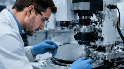
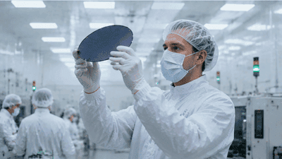
Third‑generation semiconductors push process integration in new directions, but manufacturing infrastructure remains heavily optimized for silicon. One major application scenario for silicon‑based materials is simply to maintain compatibility: using silicon wafers, carriers, or temporary bonding layers to process SiC and GaN structures in equipment originally designed for silicon.
Silicon carriers can support thin or fragile wide‑bandgap wafers during grinding, polishing, or lithography, enabling precise processing without extensive modifications to tool sets. Silicon‑compatible chemistries and consumables can be adapted to handle new materials while preserving established safety and throughput characteristics.
This process‑centric role underscores how silicon‑based materials help bridge the gap between existing fab assets and the demands of third‑generation substrates.
System‑level application scenarios: EVs, renewables, and RF infrastructure
At the system level, new application scenarios emerge where silicon and third‑generation substrates collaborate. In electric vehicles, SiC power modules coexist with silicon‑based control and sensing electronics on shared boards or substrates. Silicon provides logic, diagnostics, and connectivity, while SiC handles traction inverters and onboard chargers.
In renewable energy systems, GaN or SiC power stages interface with silicon microcontrollers, communication chips, and protection circuits in inverters or converters. Silicon‑based materials in substrates and interposers help coordinate these elements in compact, efficient units. In RF infrastructure, GaN RF devices pair with silicon RFICs and baseband chips, often interconnected through silicon‑based packaging platforms.
These system‑level scenarios show silicon’s continuing importance as the organizing material around which third‑generation devices are deployed in real‑world applications.
Future directions: deeper silicon–wide‑bandgap integration
Looking ahead, integration between silicon and third‑generation substrates is likely to deepen. More tightly coupled co‑packaged devices, silicon interposers hosting both logic and wide‑bandgap power blocks, and advanced 3D assemblies stacking silicon and SiC or GaN dies are all plausible evolutions.
Silicon‑based materials may play expanding roles in embedded thermal solutions, integrated passives, or smart sensing layers that directly interface with wide‑bandgap devices. At the same time, advances in silicon processing could make it even easier to handle non‑silicon substrates in standard fabs, further blurring the boundary between traditional and third‑generation semiconductor manufacturing.
These trends suggest that silicon’s relevance will persist, not as a competitor to wide‑bandgap materials, but as their primary partner in system design and integration.
Conclusion: silicon as the structural partner of 3rd gen substrates
Third‑generation semiconductor substrates such as SiC and GaN expand the performance frontier in power and RF devices, but they do so within systems that still rely heavily on silicon‑based materials. From GaN on Si wafers and silicon interposers to thermal structures, interface dielectrics, packaging substrates, and sensing platforms, silicon remains deeply embedded in the engineering of these new devices.
The emerging application scenarios outlined here demonstrate that silicon’s role is evolving, not disappearing. As wide‑bandgap technologies mature and spread through electric vehicles, renewable energy, and communications infrastructure, silicon‑based materials will continue to act as structural, thermal, electrical, and functional partners—anchoring third‑generation substrates within manufacturable, reliable, and intelligent systems.