Silicon-on-insulator (SOI) technology has moved from a niche substrate option to a strategic pillar in modern semiconductor design, particularly for radio-frequency (RF) and power devices. As smartphones, 5G infrastructure, connected vehicles, and advanced power management systems proliferate, the performance and integration demands placed on RF front-ends and power stages have intensified. SOI substrates, with their unique electrical and isolation characteristics, are increasingly seen as the ideal foundation for meeting these requirements. The result is a pronounced surge in demand for SOI across multiple device categories and applications.
This blog post explores why SOI substrates are gaining so much traction in RF and power devices, how their structure enables key advantages, what market and technology trends are driving adoption, and what this means for substrate suppliers, fabs, and end-system designers over the coming years.
What makes SOI different from bulk silicon
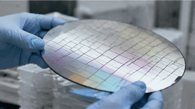
Traditional bulk silicon wafers consist of a single silicon crystal from top to bottom, with devices built directly on the surface. In contrast, SOI substrates introduce an insulating layer—typically silicon dioxide—between a thin active silicon layer and the silicon base. Devices are formed in this thin top silicon film, electrically separated from the bulk by the buried oxide (BOX).
This stacked structure fundamentally alters how electric fields and currents behave in the substrate. Parasitic capacitances and leakage paths to the bulk are reduced, substrate coupling is minimized, and device isolation is improved. These changes translate into better RF characteristics, lower power loss, and more robust performance in demanding operating environments.
For RF and power engineers, these substrate-level benefits offer a powerful lever to improve system behavior without necessarily resorting to exotic materials or radically new architectures.
SOI’s value proposition in RF front-ends
RF front-ends—comprising switches, low-noise amplifiers (LNAs), power amplifiers (PAs), and filters—must balance linearity, insertion loss, isolation, and integration density. In crowded spectrum environments, crosstalk and interference between signal paths can limit performance. SOI substrates help by providing excellent isolation between RF devices and reducing unwanted substrate conduction.
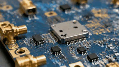
RF switches implemented on SOI can achieve low insertion loss and high off-state isolation across wide frequency bands, making them well-suited for multi-band smartphone architectures and complex 5G front-ends. The BOX layer suppresses substrate coupling, improving signal integrity even as layouts become denser.
These RF-specific advantages are a major reason why demand for RF SOI has grown steadily as wireless standards evolve and device makers seek better performance without excessive cost or complexity.
Benefits for power management and power devices
In power electronics and power management ICs (PMICs), SOI substrates offer important benefits in handling high voltages and reducing leakage. The insulating layer provides additional dielectric strength and helps confine electric fields, reducing the risk of unwanted breakdown paths through the substrate.
SOI-based power devices can achieve lower leakage currents and improved efficiency, especially in applications where devices must withstand wide voltage ranges and temperature variations. The substrate isolation also aids in integrating analog, digital, and power functions on the same die or in tightly coupled modules, by reducing interference between blocks.
As systems demand more efficient and compact power management—for example in smartphones, wearables, automotive electronics, and industrial controllers—SOI’s ability to support robust, isolated power structures becomes increasingly attractive.
Parasitic reduction and high-frequency performance
At high frequencies, parasitic capacitances and resistive paths in bulk substrates can degrade signal quality, increase loss, and complicate matching and filtering. SOI’s buried oxide layer reduces the effective substrate capacitance seen by devices, helping maintain high Q factors and cleaner RF behavior.
Reduced parasitics translate into better gain, lower noise, and more predictable impedance across frequency bands. Designers can implement RF circuits with more confidence in their models, and may achieve target performance with fewer stages or simpler matching networks.
This parasitic reduction is a key technical reason behind the soaring demand for SOI in RF applications, particularly as systems push into higher bands and more complex modulation schemes.
Isolation and integration in complex mixed-signal SoCs
Modern RF and power systems rarely consist of standalone chips; they are part of mixed-signal system-on-chip (SoC) or system-in-package (SiP) solutions that combine digital logic, analog blocks, RF paths, and power management on a shared platform. In these environments, isolation between different functional blocks is critical.
SOI substrates help maintain such isolation, reducing substrate noise coupling from digital switching into sensitive analog or RF circuits. Designers can place blocks closer together without incurring as much substrate-induced interference, enabling more compact layouts and higher levels of integration.
The ability to integrate complex functions on SOI while preserving performance is one of the core drivers behind its growing use in RF and power SoCs, particularly for space- and power-constrained applications like mobile devices and automotive electronics.
Market drivers: 5G, Wi-Fi, and beyond
On the RF side, global rollouts of 5G and the expansion of Wi-Fi standards (such as Wi-Fi 6/6E and beyond) create strong demand for advanced RF front-end solutions. These systems require more bands, more complex carrier aggregation, and tighter performance specifications, all of which stress traditional RF architectures.
SOI-based RF switches and other front-end components are well-positioned to handle these requirements. Their isolation and linearity advantages support multi-band operation without excessive loss or distortion, and their compatibility with established silicon processes helps maintain cost competitiveness.
As operators and device makers seek to deliver higher data rates and better user experiences, the underlying RF substrate choices—SOI among them—play a crucial role, boosting demand for SOI wafers and technologies.
Market drivers: EVs, renewables, and power density
On the power side, electric vehicles (EVs), renewable energy systems, and advanced industrial applications drive demand for power devices that can handle high voltages and currents efficiently. While wide-bandgap materials like SiC and GaN attract significant attention, silicon-based solutions, including SOI-based power ICs, remain essential in many segments.
SOI substrates enable robust power management ICs and driver circuits that can interface with power stages, implement sophisticated control schemes, and maintain reliability under harsh operating conditions. They also support integration of protection and sensing functions with core power control logic.
The push for higher power density, greater efficiency, and smarter control thus contributes to increasing demand for SOI, particularly in integrated power management roles across automotive and industrial electronics.
SOI vs. alternative substrate technologies
Alternative substrates, such as bulk silicon, RF CMOS on special epi structures, or compound semiconductor options, each offer their own advantages and trade-offs. Bulk silicon is well-known and cost-effective, but suffers from higher substrate coupling and parasitics at high frequencies. Compound semiconductors can deliver exceptional RF performance but often come with higher costs and integration challenges.
SOI sits in an attractive middle ground: it leverages the mature silicon ecosystem for processing and integration, while offering substrate-level isolation and parasitic reduction that narrow the performance gap with more exotic materials. For many RF and power applications, this balance of performance, cost, and integration drives a strong preference for SOI.
Consequently, as designers evaluate options for new generations of RF and power devices, SOI often emerges as a compelling choice, sustaining and growing its demand profile.
Process compatibility and manufacturing considerations
SOI substrates must fit into the broader manufacturing landscape of fabs that predominantly process bulk silicon wafers. Fortunately, many SOI technologies are designed to be compatible with existing silicon process flows, with adjustments focused on handling the thin top silicon layer and BOX-related considerations.
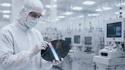
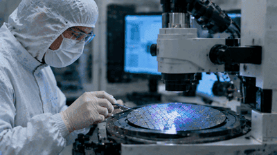
From a manufacturing standpoint, SOI wafers require careful control of top silicon thickness, BOX uniformity, and defect levels. Once these substrate parameters are well-established, device processes can be adapted without fundamental overhauls of toolsets, allowing fabs to deploy SOI-based products using much of their existing infrastructure.
This process compatibility lowers barriers to adoption, encouraging more fabs and design houses to consider SOI for RF and power products, thereby reinforcing the upward demand trend.
Supply dynamics and substrate providers
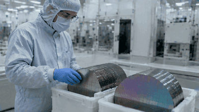
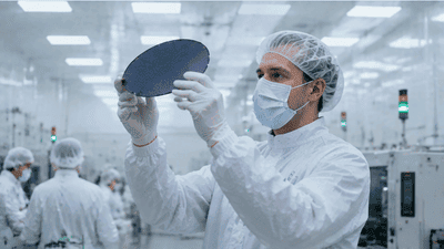
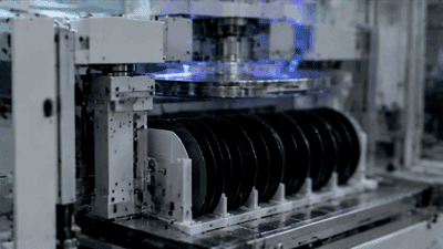
The surge in SOI demand places pressure on substrate suppliers that specialize in producing high-quality SOI wafers. These providers must manage capacity expansions, maintain tight control over wafer parameters, and support a variety of SOI flavors tailored to different applications—RF SOI, power SOI, fully depleted SOI (FD-SOI) for logic, and others.
As RF and power demand increases, substrate suppliers face the challenge of balancing volume, customization, and quality. Long-term agreements with fabs and device makers, co-development of specialized SOI platforms, and investments in new production lines become central to meeting market needs.
In some regions, localization initiatives also encourage domestic SOI capabilities, adding strategic dimensions to supply planning and contributing to a more diversified supplier landscape.
For readers interested in the overall dynamics of advanced substrates, including SOI, demand trends are broadly consistent with industry analyses of RF and power growth in the mid-2020s .
Design ecosystem and IP support
Increasing use of SOI in RF and power devices depends not only on substrate availability but also on robust design ecosystems: models, design kits, and IP blocks tuned to SOI characteristics. Device modeling must account for the BOX layer, altered capacitances, and isolation behavior, while layout rules must reflect the specific constraints and opportunities of SOI.
Foundries and EDA vendors play key roles in building this ecosystem, offering process design kits (PDKs), reference designs, and application notes that help engineers exploit SOI’s benefits without re-learning everything from scratch. Over time, the accumulation of proven IP—RF switches, LNAs, power management blocks on SOI—lowers the risk and effort of adopting SOI in new products.
This growing design ecosystem is both a consequence and a driver of SOI demand, creating a positive feedback loop between substrate adoption and design innovation.
Long-term outlook: deeper penetration and new applications
Looking ahead, the demand for SOI substrates in RF and power devices is likely to continue rising as systems become more complex and performance targets tighten. Potential new applications include increasingly integrated RF front-ends for satellite and mmWave communications, more sophisticated automotive radar and connectivity modules, and smarter power management in highly distributed energy systems.
SOI may also find expanded roles in mixed-signal and sensor-rich systems where isolation and noise control are critical, further extending its relevance beyond traditional RF and power domains. As these trends unfold, substrate innovations—such as optimized BOX thickness, engineered top silicon layers, or multi-layer SOI structures—could unlock new capabilities.
In this landscape, companies that understand and invest in SOI—from substrate suppliers and fabs to device designers—will be well-positioned to benefit from its growing importance.
Conclusion: SOI as a strategic substrate for RF and power
The soaring demand for SOI substrates in RF and power devices reflects a convergence of technical and market factors: the need for better isolation, reduced parasitics, and improved high-frequency and high-voltage performance, combined with the desire to maintain silicon-based integration and cost structures. SOI offers a powerful substrate-level solution to these challenges, enabling more capable RF front-ends and robust power management ICs in increasingly demanding systems.
As wireless connectivity expands, electric and hybrid vehicles proliferate, and energy systems grow more sophisticated, SOI is poised to remain a strategic substrate choice. Its unique blend of silicon familiarity and insulator-driven advantages ensures that the upward trajectory in demand is not a short-lived trend but part of a broader evolution in how RF and power devices are physically realized.