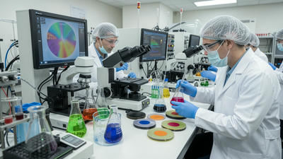
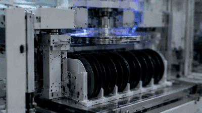
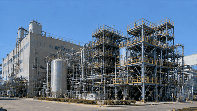
The semiconductor industry is entering a period of accelerated transformation as countries and companies increasingly focus on supply chain security, technological independence, and domestic manufacturing capabilities. Among the many semiconductor materials requiring localization, photoresists have become one of the most strategically important categories due to their direct impact on lithography performance, wafer yield, and advanced semiconductor production.
Photoresist materials represent a relatively small portion of total semiconductor manufacturing costs, but their technological importance is exceptionally high. Without high-quality photoresists, semiconductor manufacturers cannot achieve the precise patterning required for modern integrated circuits. As semiconductor processes move toward smaller geometries and more complex structures, photoresist technology has become a critical competitive factor.
A potential localization target of 20% for photoresist supply by 2026 has attracted significant attention across the semiconductor ecosystem. Achieving this goal would represent meaningful progress in reducing dependence on overseas suppliers and strengthening domestic semiconductor material capabilities. However, the path toward higher localization is complex because photoresists involve advanced chemistry, strict quality requirements, long qualification cycles, and deep integration with semiconductor manufacturing processes.
The companies that benefit most from this trend will likely be those with strong research capabilities, existing semiconductor customer relationships, advanced purification technology, and the ability to move from mature process materials toward higher-end applications.
The Strategic Importance of Photoresists in Semiconductor Manufacturing
Photoresist is a light-sensitive material used during semiconductor lithography. During manufacturing, a thin layer of photoresist is applied to a silicon wafer. The wafer is then exposed to light through a photomask, creating patterns that define the structure of semiconductor devices.
The accuracy of this process directly affects chip performance and production yield. Any defect in photoresist performance can result in pattern errors, reduced transistor reliability, or lower manufacturing efficiency.
Different semiconductor processes require different types of photoresists. These include g-line photoresists, i-line photoresists, KrF photoresists, ArF photoresists, ArF immersion photoresists, and EUV photoresists.
Each generation requires increasingly advanced material technology. While mature semiconductor processes can use relatively established photoresist technologies, advanced logic and memory manufacturing require highly sophisticated formulations with extremely low defect rates.
This technological complexity makes photoresist one of the most difficult semiconductor materials to localize.
Why Photoresist Localization Has Become a Strategic Priority
For many years, the global photoresist market has been dominated by a small number of international suppliers with decades of experience. Companies from Japan, the United States, and other regions have established strong positions through long-term cooperation with leading semiconductor manufacturers.
The concentration of supply has created concerns about semiconductor supply chain resilience. As geopolitical conditions change and semiconductor competition intensifies, controlling access to critical materials has become increasingly important.
Photoresist localization is therefore not only an economic issue but also a strategic technology issue. Developing domestic photoresist capabilities can improve supply chain stability and provide semiconductor manufacturers with additional sourcing options.
A 20% localization target would represent a significant increase in domestic participation. However, reaching this level requires progress across multiple areas, including chemical synthesis, purification technology, equipment compatibility, quality management, and customer certification.
The Current Structure of the Global Photoresist Market
The global photoresist industry has historically been highly concentrated. Leading international suppliers have accumulated decades of technical knowledge and manufacturing experience.
Their advantages come from several factors. First, they possess advanced chemical formulation capabilities. Photoresist performance depends on complex combinations of polymers, photoactive compounds, solvents, and additives.
Second, international suppliers have established relationships with semiconductor manufacturers. Qualification processes can take years because semiconductor fabs must verify that a new material does not negatively affect production yield.
Third, global leaders have invested heavily in research and development. Advanced photoresist technologies require continuous innovation to support new semiconductor processes.
Domestic companies face the challenge of competing against these established advantages while rapidly improving their own technology capabilities.
Which Photoresist Segments Are Easier to Localize?
Not all photoresist categories have the same level of localization difficulty. Mature technologies generally offer more opportunities for domestic suppliers, while advanced materials remain more challenging.
i-line and KrF photoresists represent relatively accessible segments because they have longer manufacturing histories and broader application ranges. Domestic companies have made progress in these areas by supplying mature semiconductor processes and specialty applications.
ArF photoresists represent a more difficult challenge because they require more advanced molecular design and higher manufacturing precision.
ArF immersion photoresists are even more demanding because they support advanced semiconductor manufacturing processes with strict performance requirements.
EUV photoresists represent the highest technological barrier. They require extremely advanced materials science and must meet the requirements of next-generation semiconductor production.
Therefore, the initial beneficiaries of localization are likely to be companies focused on mature and intermediate technology segments before moving toward advanced materials.
Companies With Strong Potential Benefits
Companies that benefit most from photoresist localization will likely share several characteristics: strong chemical research capabilities, semiconductor customer relationships, production experience, and the ability to achieve high-purity material standards.
Domestic semiconductor material companies with existing photoresist production capabilities are positioned to benefit because they already understand customer requirements and manufacturing challenges.
Companies involved in electronic chemicals, semiconductor materials, and advanced polymers may also gain opportunities by expanding into photoresist applications.
Those with strong research teams and experience in high-purity chemical production have advantages because photoresist development requires deep chemical expertise.
In addition, companies collaborating closely with semiconductor fabs have better opportunities to complete qualification processes and achieve commercial adoption.
The Importance of Semiconductor Customer Certification
One of the biggest challenges for photoresist localization is customer certification.
Semiconductor manufacturers cannot immediately replace existing photoresist suppliers because materials are deeply connected with manufacturing processes. A change in photoresist formulation can affect exposure performance, etching behavior, defect rates, and final chip quality.
As a result, new suppliers must complete extensive testing before achieving mass production approval.
This process can take several years, especially for advanced semiconductor applications.
Companies that have already entered semiconductor production lines have a significant advantage because they have accumulated manufacturing data and customer trust.
Technology Challenges Facing Domestic Photoresist Companies
Although localization opportunities are growing, several technical challenges remain.
The first challenge is achieving ultra-high purity. Semiconductor manufacturing requires extremely low contamination levels because even tiny impurities can affect chip performance.
The second challenge is improving resolution capability. As semiconductor features become smaller, photoresists must support increasingly precise pattern transfer.
The third challenge is improving consistency. Semiconductor manufacturers require stable performance across thousands of production batches.
The fourth challenge is developing complete material ecosystems. Photoresist performance depends not only on the resist itself but also on related materials, processing conditions, and equipment compatibility.
Overcoming these challenges requires continuous investment in research and manufacturing infrastructure.
The Role of Government and Industrial Support
Government support and industrial investment are important factors accelerating semiconductor material localization.
Developing advanced photoresist technology requires long-term investment because research cycles are lengthy and commercial returns may take years.
Support programs can help companies build production facilities, improve research capabilities, and establish partnerships with semiconductor manufacturers.
However, long-term competitiveness depends on technological achievement rather than policy support alone. Semiconductor customers ultimately prioritize performance, reliability, and cost efficiency.
Impact on Semiconductor Supply Chains
Higher photoresist localization will reshape semiconductor supply chains by creating more diversified sourcing options.
For semiconductor manufacturers, additional suppliers can reduce supply risks and improve operational flexibility.
For domestic material companies, localization creates opportunities to increase market share and develop stronger technology capabilities.
For international suppliers, increasing competition may encourage faster innovation and improved customer cooperation.
The overall result could be a more balanced and resilient semiconductor material ecosystem.
Investment Opportunities and Market Outlook
The photoresist localization trend creates several investment themes across the semiconductor materials industry.
The first opportunity lies in companies already producing semiconductor-grade chemicals and materials. These companies have existing manufacturing capabilities and can expand into photoresist applications.
The second opportunity lies in companies developing advanced polymer and chemical technologies. Photoresist innovation depends heavily on materials science.
The third opportunity lies in suppliers supporting semiconductor manufacturing ecosystems, including purification equipment, testing services, and process solutions.
However, investors should recognize that photoresist development is a long-term process. Commercial success depends on technical breakthroughs, customer qualification, and sustained manufacturing performance.
Future Development Toward 2026 and Beyond
By 2026, photoresist localization is expected to make meaningful progress, particularly in mature semiconductor applications.
Domestic suppliers are likely to increase market share in i-line, KrF, and selected ArF applications as manufacturing capabilities improve.
Advanced photoresists, especially EUV-related materials, will remain a longer-term challenge requiring additional research and development.
The semiconductor industry will continue moving toward greater supply chain diversification, and photoresist will remain one of the most important areas of competition.
Companies that successfully combine chemical expertise, semiconductor knowledge, and customer cooperation will have the strongest opportunities to become future industry leaders.
Conclusion
The goal of achieving a 20% photoresist localization rate by 2026 reflects the growing strategic importance of semiconductor materials. While photoresist represents only a small percentage of semiconductor manufacturing costs, its role in determining chip performance and production reliability is enormous.
The biggest beneficiaries of this trend will likely be companies with strong chemical technology foundations, semiconductor customer relationships, and the ability to achieve high-quality manufacturing standards.
Localization will not happen overnight, especially in advanced photoresist technologies. However, continued investment, technological improvement, and cooperation between material companies and semiconductor manufacturers are creating a path toward a more diversified semiconductor supply chain.
As global semiconductor competition intensifies, photoresist technology will become an increasingly important strategic capability, and the companies that successfully overcome technical barriers may become key players in the next generation of semiconductor manufacturing.